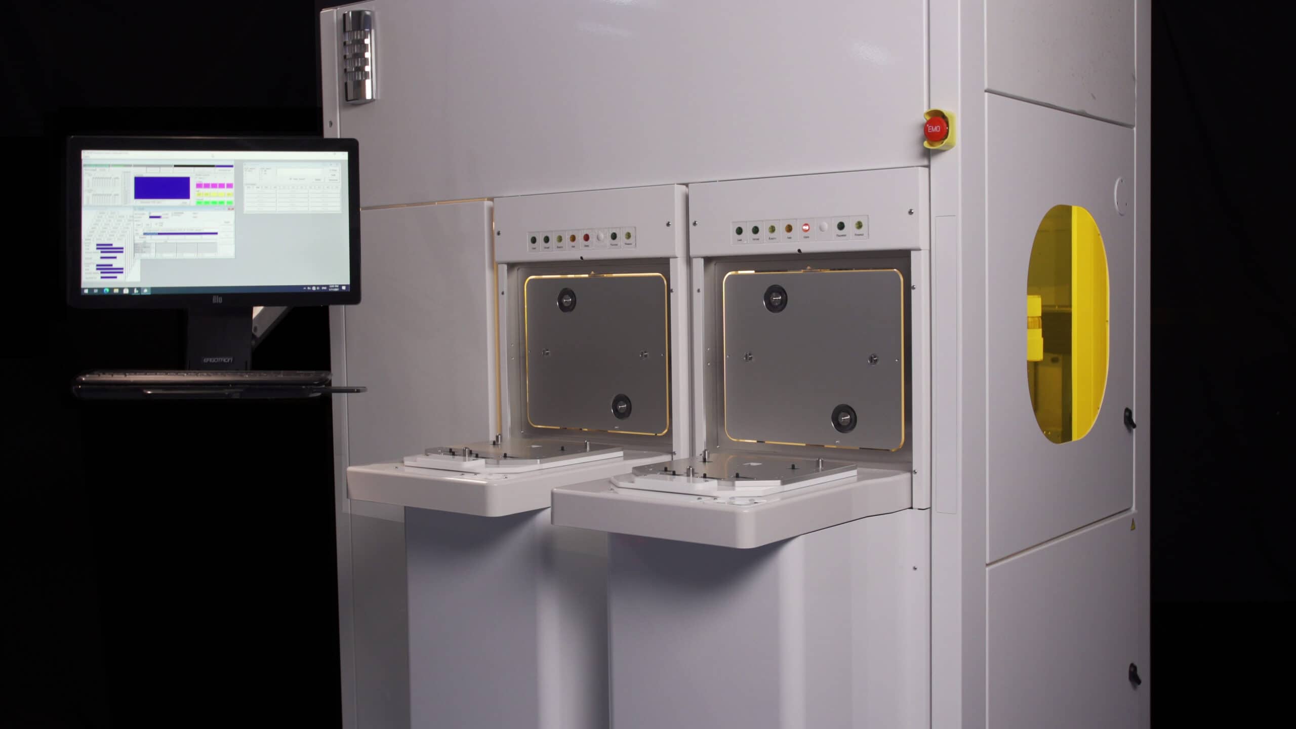
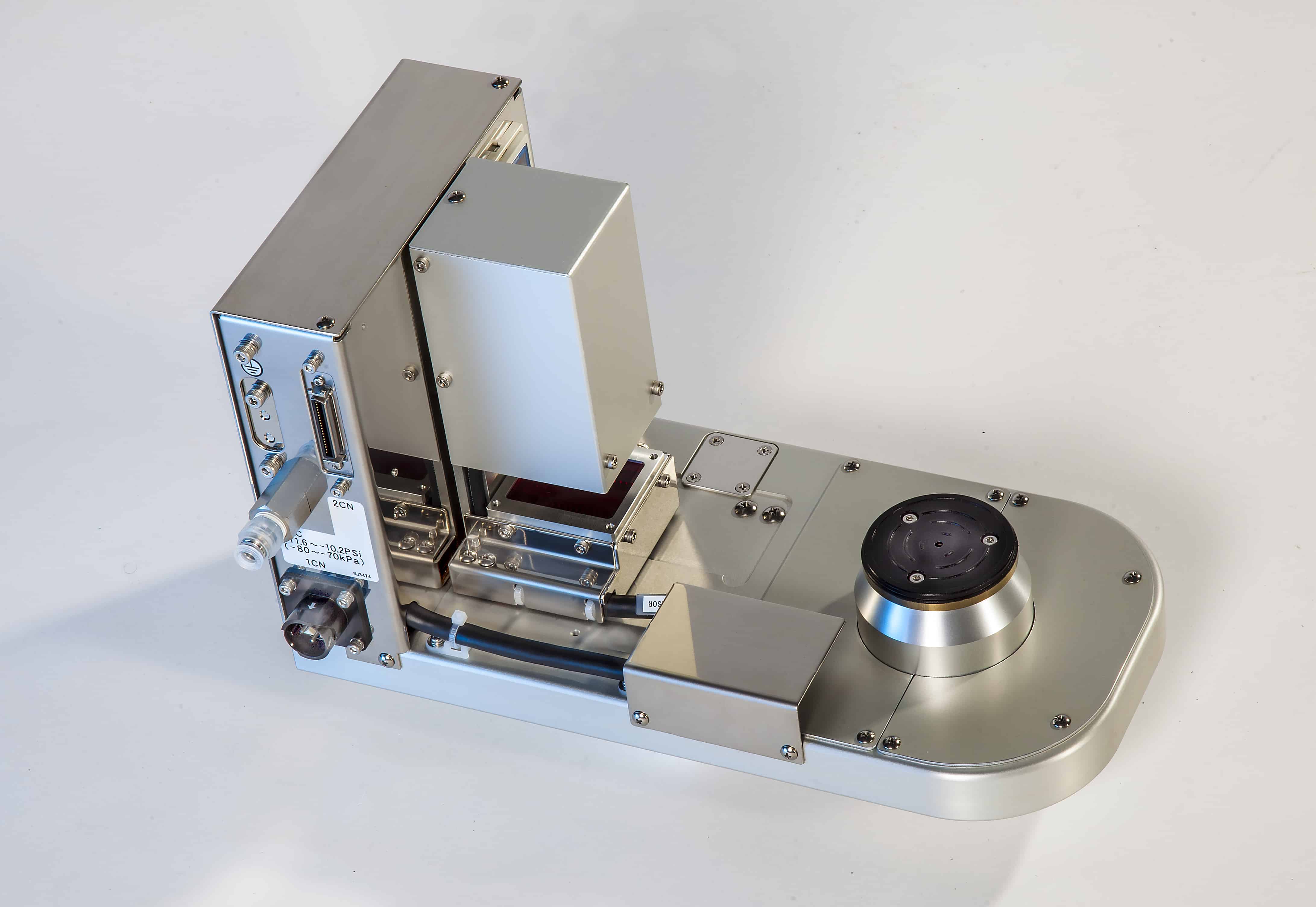
Traditionally, semiconductor facilities have relied on handling systems optimized for a single wafer size, limiting flexibility and adaptability in production processes. However, a new frontier emerges with the advent of dual-size wafer handling solutions, a game-changing feature that promises to revolutionize the industry. At the forefront of this innovation is the introduction of Yaskawa's Dual-Size Wafer Handling Bridge Tool, a pioneering advancement that enables semiconductor manufacturers to seamlessly integrate two different wafer sizes within the same handling system. This breakthrough not only streamlines production workflows but also enhances efficiency, scalability, and cost-effectiveness in semiconductor fabrication. As we embark on this exploration, we unveil the transformative potential of dual-size wafer handling and its profound impact on semiconductor manufacturing.
Understanding the Variations in Wafer Sizes and Their Handling Requirements
In semiconductor fabrication, the diverse landscape of wafer sizes presents a variety of challenges for manufacturers. While most tools are designed to accommodate a single wafer size, the demand for flexibility has led to the emergence of dual-size wafer handling solutions.
Traditionally, semiconductor facilities standardized their processes around specific wafer sizes, such as the common 200mm or 300mm wafers. However, as the industry evolves and customer requirements become more diverse, the need for handling both 200mm and 300mm wafers concurrently has become increasingly frequent.
This dual-size wafer handling capability offers semiconductor manufacturers the flexibility to adapt to changing production needs, optimize equipment utilization, and streamline workflow efficiencies.
Yet, with this flexibility comes complexity, as designing equipment to seamlessly handle different wafer sizes while maintaining precision and reliability poses significant engineering challenges.
Challenges in Dual-Size Wafer Handling
Handling dual-size wafers presents semiconductor manufacturers with a unique set of obstacles that must be navigated with precision and ingenuity. At the forefront of these challenges is the complexity of designing equipment capable of accommodating multiple wafer sizes seamlessly. Unlike single-size handling systems, which are optimized for specific dimensions, dual-size wafer handling requires a delicate balance between versatility and precision. Ensuring that handling mechanisms, clamps, and transfer systems can securely grip and manipulate both 200mm and 300mm wafers without compromising accuracy or reliability demands meticulous engineering and rigorous testing. Additionally, the intricacies of alignment and positioning become magnified when dealing with dual-size wafers, as variations in dimensions, thicknesses, and orientations must be carefully managed to maintain process consistency and yield optimization.
Addressing Customization Requirements
In the dynamic realm of semiconductor manufacturing, addressing customization requirements in wafer handling equipment is paramount to ensuring optimal performance and efficiency. One of the key customization considerations revolves around the loading media used, whether it be Front Opening Unified Pods (FOUPs), cassettes, or Standard Mechanical Interface (SMIF) pods. Each loading media presents unique challenges and demands tailored handling mechanisms to facilitate seamless wafer transfer. Moreover, the precise execution of GET/PUT operations from and to the loading station requires meticulous attention to parameters such as End Effector (EE) design, pitch, and gripping techniques to guarantee smooth workflow and minimize the risk of wafer damage. Alignment accuracy is another critical aspect, as achieving precise wafer alignment is essential for subsequent processing steps and overall product quality. Additionally, Optical Character Recognition (OCR) capabilities play a crucial role in reading vital information imprinted on wafers, such as identification codes and orientations. Furthermore, some processes necessitate wafer flipping during handling, requiring reliable flipping mechanisms to ensure proper orientation.
Adapting OCR Technology for Varying Wafer Sizes
Another significant challenge in the realm of semiconductor manufacturing is the need for the automatic adjustment of Optical Character Recognition (OCR) technology according to the size of the wafer. As facilities handle wafers of different dimensions, particularly the common 200mm and 300mm sizes, the precision in OCR technology becomes crucial. This technology must dynamically adjust to accurately read and process information from wafers of varying sizes without manual intervention. The ability to automatically recalibrate the OCR reader enhances the efficiency of the manufacturing process, reduces potential errors, and ensures a smoother workflow.

Yaskawa's Bridge Tool EFEM: Meeting Industry Needs
Yaskawa's Bridge Tool EFEM stands as a testament to innovation and excellence in semiconductor manufacturing, offering a comprehensive solution to meet the diverse needs of the industry. This sophisticated tool plays a pivotal role in streamlining wafer handling processes, ensuring efficiency, precision, and reliability at every stage of production. With a keen understanding of the challenges faced by semiconductor manufacturers, Yaskawa's solution is meticulously designed to overcome these obstacles and optimize operational workflows.
From accommodating different wafer sizes to addressing customization requirements such as loading media compatibility, alignment accuracy, and OCR capabilities, Yaskawa's Bridge Tool EFEM excels in delivering unparalleled performance and functionality.
Essential Features of the Handling Bridge Tool: Streamlining Semiconductor Manufacturing
The Handling Bridge Tool embodies a suite of essential features designed to streamline semiconductor manufacturing processes with precision and efficiency. At its core are three key components: station name designation, customizable parameters, and detailed mapping functionalities. The automatic designation of station per wafer size facilitates seamless integration and troubleshooting. By assigning specific functions to each handling station within the tool, this approach simplifies operational processes and minimizes downtime. Customizable parameters allow users to fine-tune handling operations according to specific process requirements, ensuring optimal performance and adaptability to changing production needs. Additionally, detailed mapping functionalities enable precise coordination between the Handling Bridge Tool and other manufacturing equipment, facilitating smooth workflow transitions and enhancing overall productivity.
Conclusion: Embracing Innovation in Semiconductor Manufacturing
Innovation continues to drive progress in semiconductor manufacturing, with advancements in wafer handling technology playing a pivotal role in shaping the industry's trajectory. The demand for flexibility and efficiency in production processes has led to the emergence of dual-size wafer handling solutions, offering semiconductor manufacturers unprecedented versatility in accommodating different wafer sizes within their operations. This innovative approach not only streamlines workflows but also enhances productivity and cost-effectiveness, enabling manufacturers to meet the evolving demands of the market with agility and precision. As the industry evolves, collaboration and innovation will remain essential in addressing the diverse challenges and opportunities that lie ahead.


