

From Circular to Rectangular
Transforming Substrate Handling in Semiconductor Manufacturing
Introduction: the Evolution Beyond Traditional Wafer Shapes
-
The semiconductor industry has been defined by circular wafer formats for decades, evolving from 2-inch diameter wafers through to today's industry-standard 12-inch (300mm) wafers (leaving aside the attempt to go for 450mm wafers – 18” – that started in 2008 and ended in 2018). However, the explosive growth of advanced packaging technologies and artificial intelligence applications is driving a paradigm shift toward rectangular substrates, representing a fundamental departure from traditional manufacturing approaches.
This transition addresses critical limitations in material utilization and design flexibility that have constrained innovation in next-generation semiconductor devices. Rectangular substrates promise to reshape production methodologies and equipment design across the semiconductor ecosystem.
Understanding the Transition to Rectangular Substrates
Rectangular substrates under consideration typically span dimensions of 510x515mm and 310x310mm, formats specifically optimized for advanced packaging applications and AI chip manufacturing requirements. The driving force behind this transition lies in advanced packaging technology and AI applications, where traditional circular wafer constraints have become increasingly problematic.
AI chips, with their complex multi-die architectures and heterogeneous integration requirements, demand substrate formats that can accommodate diverse component layouts without circular boundary limitations. Advanced packaging applications, including System-in-Package (SiP) and chiplet integration, similarly benefit from the design freedom that rectangular substrates provide.
Traditional circular wafers inherently create unusable peripheral areas when rectangular or square dies are arranged within their boundaries, resulting in significant material waste and reduced yield efficiency—particularly pronounced in advanced packaging applications.
Potential Advantages of Rectangular Substrates
Increased Usable Area: Rectangular substrates eliminate geometric mismatch by providing a format that naturally aligns with standard die shapes, resulting in a dramatic improvement in usable surface area and increased die yield per substrate.
Advanced Chip Packaging Benefits: The rectangular format provides geometric freedom necessary to accommodate complex multi-die arrangements, enabling more efficient interconnect routing, optimized thermal management, and improved signal integrity in advanced packaging applications.
Reduced Waste: Environmental and economic benefits extend beyond material savings, reducing raw material consumption and waste disposal requirements while improving manufacturing economics.
Critical Challenges in Implementation
Transitioning from circular to rectangular substrates presents a multi-dimensional challenge that impacts nearly every aspect of semiconductor manufacturing infrastructure. Existing fab environments are deeply optimized around circular wafer handling, and adopting rectangular panels introduces both mechanical and system-level complexities.
Material Handling Infrastructure:
OHT (Overhead Transport) systems will require redesigned carriages to support the altered shape, size, and weight distribution of rectangular substrates. In tandem, stocker units must be modified to accommodate these new carriages, ensuring smooth material flow across the fab.
Tool Interface Redesign:
Sorters, typically configured for round wafers, must be re-engineered to manage rectangular formats efficiently. A completely new load port will be needed—one capable of handling new cassette shapes while ensuring compatibility with critical features such as mapping capabilities and Cassette ID Readers (CID).
Equipment Front-End Module (EFEM):
The EFEM architecture will likely undergo significant changes in both size and configuration. Rectangular substrates may require customized end-effector designs, updated aligners, and modified substrate flow control. For instance, pre-aligners will need to be redesigned to support edge orientation and flat detection on non-circular geometries, while maintaining high alignment accuracy.
Automation & Communication Protocols:
Fab automation software such as SECS/GEM may require updates to support new substrate formats and device IDs, along with expanded parameter sets and handling sequences. In addition, these changes may necessitate new hardware, including updated cables, connectors, and interface modules to support the broader range of mechanical and software requirements.
This transformation is not merely a tooling change—it redefines entire workflows and requires close coordination across equipment vendors, fab automation teams, and process engineers to ensure a seamless shift toward rectangular substrate adoption.
Yaskawa’s Advanced Solutions for Rectangular Substrates
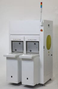
Yaskawa's comprehensive approach addresses rectangular substrate handling challenges through the SEMISTAR-GEKKO series, a breakthrough technology specifically developed for the semiconductor industry's unique demands.
Yaskawa developed a special EFEM solution to address these new challenges. This newly designed EFEM features dimensions optimized for handling the rectangular substrates between critical stations such as the Aligner, OCR, and Flipping units, as well as the host station. It integrates an additional array of sensors to support advanced calibration and fine-tuning of the system, ensuring the highest alignment accuracy for non-circular geometries. Beyond the hardware, the EFEM’s software capabilities were also upgraded, providing enhanced adaptability and control tailored to the demands of rectangular substrate handling.
Within this broader solution, the SEMISTAR-GEKKO series plays a pivotal role:
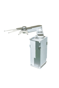
Revolutionary Technology: Key models, including the MU113 and MD124D, have been meticulously designed to handle 510x515mm and 310x310mm rectangular substrates dominating advanced packaging and AI chip applications.
Breakthrough Passive Grip Technology: At the heart of the GEKKO series lies Yaskawa's revolutionary Wafer Passive Grip technology, enabling significant reduction of wafer stress while delivering cleaner gripping signatures. This technology is crucial for rectangular substrates, where corner and edge vulnerabilities demand exceptionally gentle handling approaches.
Advanced Motion Control: The GEKKO series incorporates unique Motion Algorithms specifically optimized for smooth rectangular substrate delivery. This sophisticated control system addresses asymmetrical mass distribution challenges, ensuring stable and precise handling during high-speed operations while compensating for uneven weight distribution and potential oscillation tendencies.
Precision Engineering: The series eliminates vibration through direct drive YASKAWA motors, delivering improved stopping and absolute position accuracy. Advanced acceleration and deceleration control enables high-speed transfers while maintaining gentle handling characteristics essential for preventing damage to vulnerable substrate areas.
Intelligent Control Systems: The Advanced SR200 Controller coupled with user-friendly smart robot pendant provides intuitive control over complex rectangular substrate handling operations, with adaptive protocols accommodating variations in substrate dimensions and materials.
Versatile Configurations: Beyond passive grip technology, the GEKKO series offers optional vacuum and edge grips specifically designed for rectangular substrate applications, plus various robot options including Vacuum, Anti-corrosion, and Long Z configurations for diverse fab environments.
Conclusion: Embracing the Rectangular Substrate Revolution
The transition to rectangular substrates represents a fundamental evolution reshaping advanced packaging and AI chip production methodologies. With 510x515mm and 310x310mm formats becoming increasingly prevalent, this transformation addresses critical limitations constraining next-generation semiconductor applications.
Yaskawa’s comprehensive approach combines its newly designed EFEM system—optimized for precise substrate transfer, advanced calibration, and upgraded software capabilities—with the SEMISTAR-GEKKO series, which introduces revolutionary Passive Grip technology, advanced motion algorithms, and precision engineering. Together, these solutions create a robust, end-to-end platform for managing the complexities of rectangular substrate. As the semiconductor industry evolves in response to advancing AI applications and sophisticated packaging demands, rectangular substrate handling represents a critical capability enabling manufacturers to achieve new levels of efficiency, flexibility, and innovation. Yaskawa's comprehensive GEKKO solution demonstrates that embracing rectangular substrate technology is essential for the future of semiconductor manufacturing, where advanced packaging and AI chip production define the industry's trajectory.